Global Navigation Satellite Systems Software-Defined Receivers explained. Part 0: Hardware and system design
In this series of articles I’d like to share my experience in GNSS receiver design over the last 10+ years. Writing down the knowledge on various topics is an excellent way to share the information, as well as structuring and preparing this kind of educational material allows one to find the missing pieces in one’s knowledge.
I’d like to start from a system design perspective since most of the decisions made at this stage are directly influencing the type of processing that will be used later.
- Part 0: Hardware and system design
- Part 1: Digital frontend
- Part 2: Jamming mitigation
- Part 3: Acquisition
- Part 4: Correlation and tracking
- Part 5: Standalone positioning
- Part 6: Advanced positioning methods
Overview
A general schematic of the GNSS receiver is presented below with the high-level blocks. Generally, the plurality of the satellite signals is received in an antenna (or multiple antennas), filtered, amplified and then fed into the (multiband) radio-frequency (RF) frontend to convert the signal into the baseband.
The baseband signal is quantized and sampled in the ADC and then processed by the digital frontend, acquisition engine, correlation engine, tracking loops etc. The tracking loop results are used to generate the observables and with (optional) external data the receiver performs the positioning routines. On top of that, there is a user interaction like position, velocity and time (PVT) and observables data output, generation of the synchronized timescale pulses, various external events registration and so on.

To be honest, with all the receivers I’ve made over the last decade, the system design was by far my favourite stage of development. It involves a lot of research and communication with the potential customers, handling of both software and hardware aspects, like PCB, mechanical, environmental, not to say the RF and electrical.
Hardware
The system design starts with collecting all the requirements and limitations for the future receiver, which will result in some related decisions. For example:
- We need to build an accurate heading solution → we’ll have to build a receiver with two antenna inputs → we need a multi-channel RF-frontend and a baseband processor with enough processing power
- We are limited to a special ASIC or FPGA family (this happens, when you need to use the in-house solution) → depending on the supposed use cases we should choose the appropriate RF frontend, inspect it with an evaluation kit and propose a frequency plan and a functional diagram of the receiver
- We have to comply with the certain form-factor either by legacy reasons or if we want to propose a hot-swap for some competitor → we should carefully inspect all the tolerances and limits (mechanical, electrical and thermal) and check for the undocumented behaviour of the reserved pins.
One of the interesting topics is the selection of an appropriate antenna. There are three kinds of antennas:
- Passive antennas, are often used in trackers, smartphones and other cost-effective solutions. There’s a great application note (GNSS antennas. RF design considerations for u-blox GNSS receivers. Application note) by u-blox.
- High-precision active antennas, with built-in filters and amplifiers and, most importantly guarantee a stable phase centre position. As you may know, all the positioning and signal processing is performed for the signals, received at the phase centre of an antenna. When the phase centre is stable, signals from the satellites at various elevation angles are perceived at the same virtual position. An excellent overview of the active antennas is provided in a whitepaper (Topcon GNSS Reference Station with Cavity Filters TPS CR-G5-C & TPS PN-A5-C) by Topcon Positioning Systems with a major focus on the cavity filters.
- Antenna arrays with null- and beam-formers. This is a deep and interesting topic, check out the NovAtel GAJT-710 antenna, I’ll briefly explain the antenna array algorithms in the antijamming section.
Active antennas, due to the presence of an amplifier, require additional power to operate properly. This is solved (quite elegantly) by providing the DC via the same signal coaxial cable. The DC flows from the receiver (or the bias tee) to the antenna and the RF signal comes the other way around.
The signal from the antenna in the receiver is amplified with an onboard LNA to compensate for the signal losses in the cable. Then, after additional signal splitting and band-dependent filtering, the signal is processed in the RF frontend. The goals of the RF frontend are the following:
- Additional signal amplification with automatic gain control (AGC)
- Signal spectrum shift to the baseband frequency
- Additional signal filtering
- (Optional) Signal sampling with onboard ADCs
The first gain-controlled amplifier, which is often omitted in the low-end frontends is required when the interference is present. As you may know, the mixer is a non-linear device that multiplies the input signal with a reference signal to produce a signal with a set of sum and difference of the original frequencies. However, to operate correctly, the powers of both signals should be similar. If this condition is not met the major signal distortion will be observed.
There’s a way to overcome this issue with an approach, usually found in RADARs, called the bandpass sampling. It’s based on the properties of the digital signal and allows to use of the ADC as a perfect mixer. There’s an article I’m happy to share or discuss where I demonstrate that with sufficient amplification this approach is equivalent and even surpasses the traditional RF frontends in terms of positioning precision.
Nowadays it’s common to have all the functions of the frontend in a single RF integrated circuit. This approach allows to reduce the footprint of the receiver, simplify the overall design and reduce the cost both of the receiver itself and the R&D expenses. There are two major players in COTS (commercially available off-the-shelf) RF frontends: Maxim Integrated (now part of Analog Devices) with MAX2769/MAX2771 chips and NTLab with NT1065/NT1066/NT1062 device family. Let’s illustrate a hardware part of the L1/L2 receiver:

Frequency plan
When the hardware system design is more or less determined, it’s time to estimate the frequency plan, which defines the set of parameters responsible for the satellite signal processing. It includes:
- Reference oscillator frequency $f_{ref}$
- Sampling rate $f_s$
- Local oscillator (LO) frequencies $f_{LO_i}$
- Resampling factors in the digital frontend
The key point to the frequency plan design is to distribute and allocate the signal spectrum in a manner to avoid spectrum overlapping, which is often referred to as aliasing. This should take into account all the frequency shifts in RF and digital frontends, as well as resampling. The tricky part here is that when it comes down to the real hardware there are a lot of limitations like integer PLLs (hence, a finite set of local oscillator frequencies), sampling rate and bandwidth limits, presence or lack of the I/Q processing in the baseband processor and so on. For example, here’s an illustration of the frequency plan for the one of my first receivers:
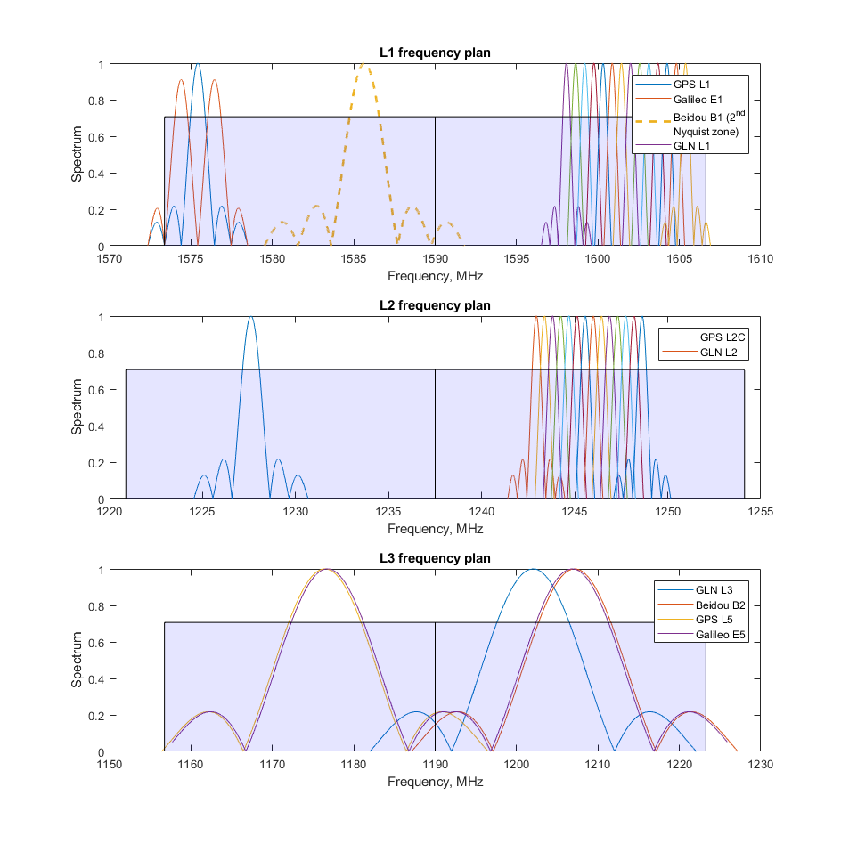
It was built with two NT1065 RF frontends to cover the L1/L2/L3/L5 GNSS signal bands and had local oscillators at 1590, 1237.5 and 1190 MHz. The fourth local oscillator was set to 1330 MHz and was a source of the 66.5 MHz ADC clock.
One more important thing is that the frequency plan should not be treated as something engraved in stone: it may (and should) change to reflect the situation. One of the best things about the modern IC-based RF frontends is their reconfigurability: if the selected ADC clock or the LO frequency doesn’t fit you for some reason (unexpected spectrum harmonics from the self-interference is one of the possible problems) it’s easy to use another configuration with a different set of register values.
Summary
This introductory part is a very high-level overview of the system design process for the GNSS receivers, but this is the kind of knowledge you get from experience and have to acquire piece by piece from multiple sources. As I’ve mentioned, it always was my favourite design stage since it always represented pure research and, in a matter of speaking, art.
There’s also a big part of the system design related to the mechanical specifications, external data and user interaction, I hope to add it once I revisit this text.