NT1066 Florea preliminary review
UPDATE: Check out the hands-on review.
As you may know, our MC149.01 GNSS receiver is built upon two NTLab NT1065 front-ends. The task of the front-end is simple, yet crucial for the receiver quality. It amplifies the signal, translates it from the radio- to the intermediate frequency (~1.6 GHz to ~10 MHz), filters it and, optionally, quantizes with an internal ADC onboard.
Unfortunately, due to the limitations of the NT1065, we were forced to use two chips and use only 1.5 of them, like in the schematic below:
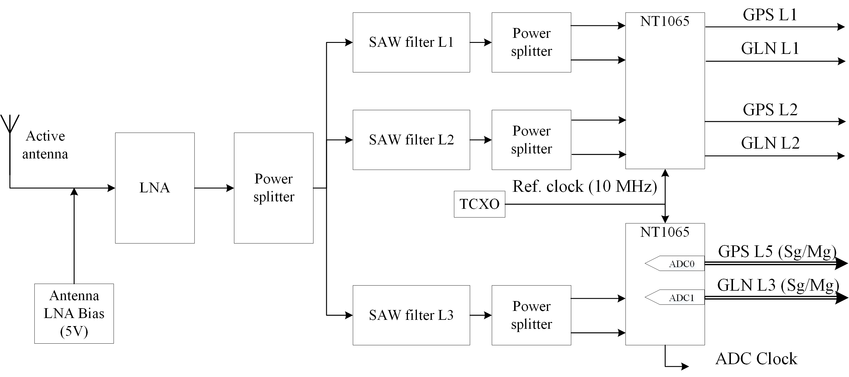
The main complaint here is the lack of the ability to cover all three GNSS bands with one chip. Another minor disappointment is that you can’t sync ADCs from one chip with the clock from another. This lead to this kinda strange solution with the L3 signals being quantized onboard and L1/L2 transferred as analog signals and digitized in the internal 10-bit ADC of the BBP2 SoC.
Earlier this year at the Navitech expo I’ve had a little chat with NTLab’s CEO Dmitri Tcherniakovski about their new design and he sent me some preliminary documentation. I’ve decided not to write anything prior to the NTLab website, and when they finally published the information, I’m very glad to share my thoughts.
New front-end is more flexible with three wideband channels and one narrowband. Wideband ones are pretty similar to the ones NTLab used in their prototype GNSS front-end NT2024 and the narrow one in exactly the same as in the previous chip.
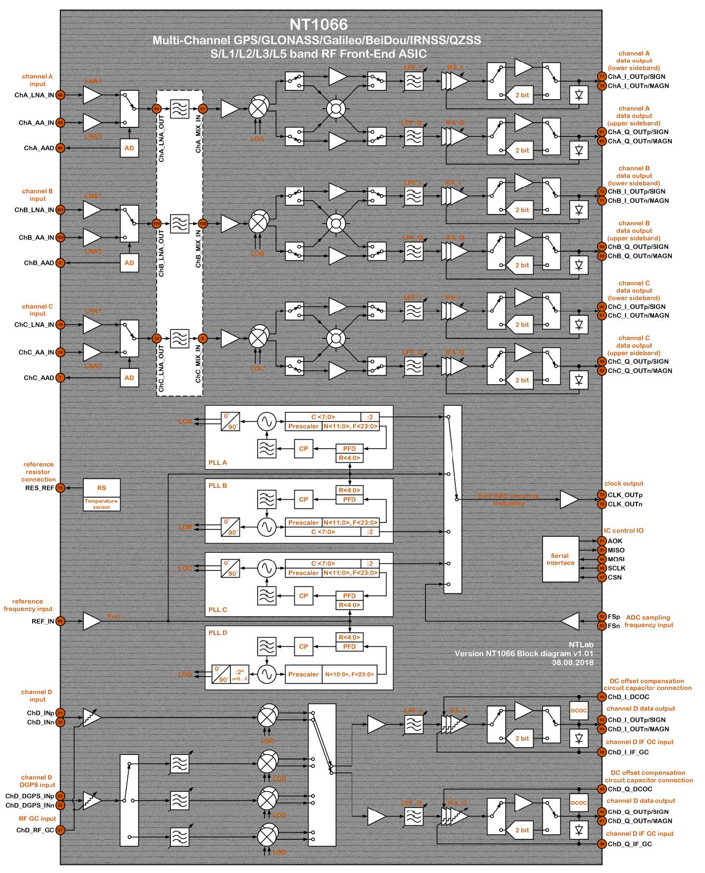
The core (and the best) feature is the ability to get quadrature (I/Q) signal, which allows cutting the sampling frequency in half. The only drawback in the complex sampling is that the ADCs should be perfectly synced to mitigate the effects of the quadrature imbalance, but this is yet to check when I’ll get my hands on the evaluation board.
The other thing I really like is the NT2024-derived possibility to use fractional-N in the oscillators’ PLL. This is a degree of freedom that I really missed in the NT1065.
NT1066 allows you to use wideband channels in several ways, based on the low-pass filters and commutation:
- IQ mode
- Sideband modes, in which one of the outputs is disabled
- Independent mode, in which I and Q outputs produce independent sidebands (useful to separate signals)
With all said and done our MC149.01 receiver can be simplified to the following schematic:
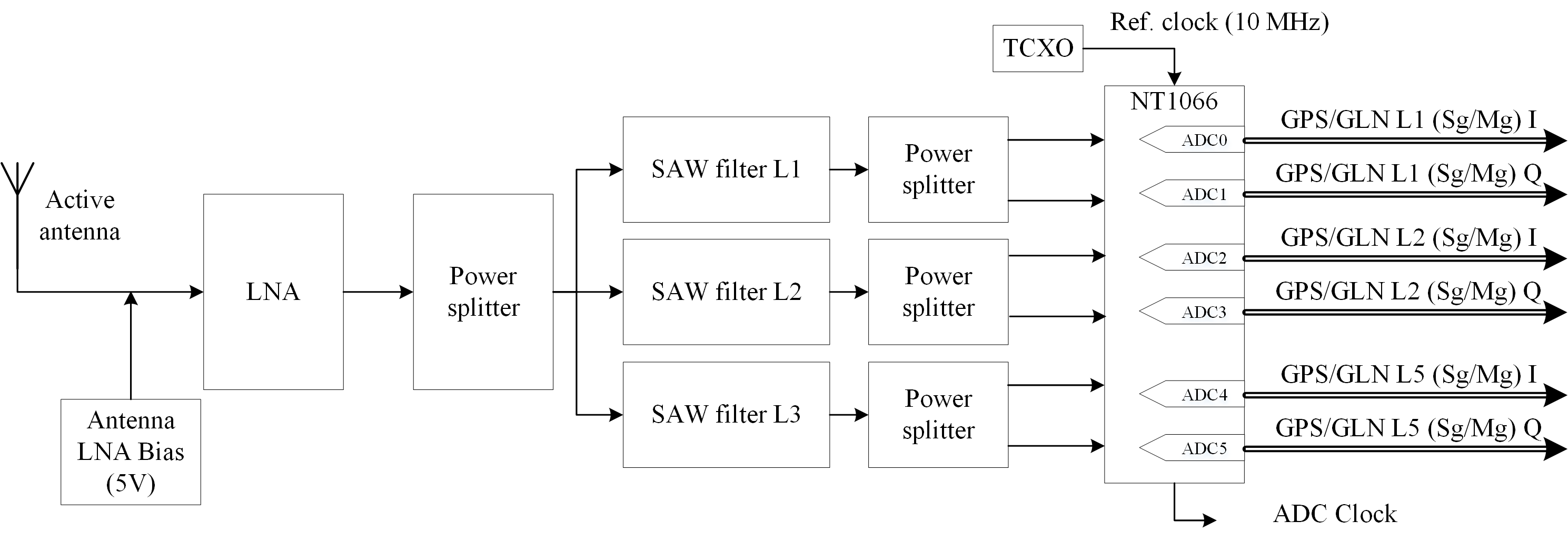
It will allow us to disable the ADCs in our ASIC, save a lot of space in the RF signal chain and even improve the SNR.
There are still, however, several things to experiment with when I’ll get my hands on the evaluation board:
- Check the phase response of the low-pass filters, especially in the I/Q-mode;
- Check for the I/Q phase imbalance and quadrature sampling quality
- Get pretty correlation peaks to write another article
The good thing is, as it seems to me now, we would be able to quickly substitute the two NT1065 chips with one of those with minimal modifications to the receivers’ software and no changes to the frequency plan whatsoever!
P.S. There is a work-in-progress control library, feel free to give any feedback, use and modify it.